SK Infrared is developing high-performance, photonic detectors based on Type II Superlattices (T2SL), purpose built for their applications. Our devices are custom built to serve unique customer needs for specific applications, and finely tuned to generate the required information.
Technology
SK Infrared is involved in the development of next-gen infrared imagers and can fabricate test diodes with 320×256 focal plane arrays as well as 640×512 fpa imagers using Type II strained layer superlattices.
This technology has demonstrated dramatic improvement in device performance in the past few years.
The SLS technology consists of hundreds of periods of very thin layers of two different semiconductors. Specifically, InAs and GaSb are deposited one after the other. This idea was first proposed by Nobel Laureate, Leo Esaki, in the early 70’s. However, the technology did not exist to actually realize these highly precise nanostructures in the laboratory.
In the past decade, there has been a dramatic improvement in the performance of infrared imagers based on these superlattices. The superlattices have been identified as a leading technology for the development of next generation infrared imagers by the Department of Defense. They have a large quantum efficiency and high sensitivity in the mid wave infrared (3-5µm) and long wave infrared (8-12µm).
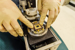 We have access to “Epi to Camera” research for realizing these detector technologies. This involves heterostructure design and engineering, crystal growth using molecular beam epitaxy, materials characterization, single and focal plane array fabrication, hybridization and radiometric characterization.